


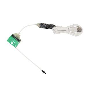
 1.0mm Endoscope
1.0mm OCHTA10 Professional HD Waterproof Endoscope
- 2.5mm Endoscope
1500×1500 2.5mm OCH2B10 Medical Endoscope Camera
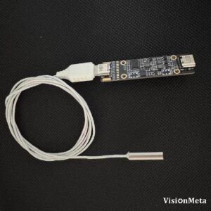
- 1MP Endoscope
Mini 3.1mm Medical Endoscope ES101 Endoscope
- 1.4mm Endoscope
1.4mm OCHTA10 Tiny Endoscope Module USB Industrial Medical
- 1.8mm Endoscope
1.8mm/2.0mm OCHFA10 Medical Endoscope 720*720 518 Kpixel 60fps
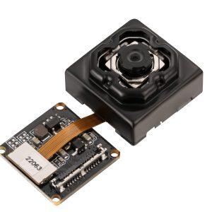
- 12MP Camera Module
5MP/12MP Flexible Spilted FPC Camera Module USB AF/FF/MF
- 12MP Endoscope
12MP 4K IMX258 15.0mm HD Digital Mic Endoscope Borescope
- 1MP Endoscope
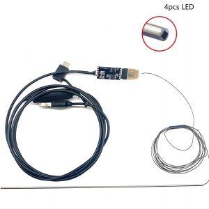
1MP 3.3mm OH01A10 Micro Endoscope 60fps LED for Medical
- 2MP Camera Module
2MP 3.0mm OV2740 Micro USB Endoscope Module 160° FOV
- 1.8mm Endoscope
1.8mm OV6946 Endoscope Module USB Decoder Industrial Medical
- 13MP Camera Module
13MP Mini Camera Module IMX258 Optical Image Stabilization
- 4K Camera Module
12M iCatch V39M 3-Axis Anti-Shake EIS Gimbal Camera Module for Drone
- 5MP Camera Module
5MP 1/4″ OV5648/OV5645/OV5640 MIPI Auto Focus Camera Module
- 13MP Camera Module
13MP IMX258 1/3.06 Inch HD 4K USB Camera Module
- 2MP Camera Module
2MP 1/2.7″ PS5268 Dual Lens Face Recognition Camera Module
- 1.4mm Endoscope
1.4/1.8mm OV6948 Endoscope Medical Camera Module FOV 120°
- 2MP Endoscope
2MP 5.0/5.2/5.5/6.0mm OV2740 Endoscope Module 60fps


Views: 226
Real superb info can be found on site.Raise range